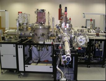
Nanotechnology complexes (NTC) Nanofab 100 have modular design and can be used both for research purposes in various fields of nanotechnology (microelectronics and nanoelectronics, Nano photonics, Nano materials and etc. ) and for low-batch production of nanostructure, nanoelements and nanodevices.
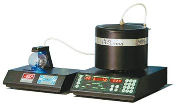
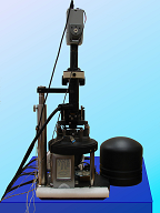
CVDomna can be used both in research work and in the educational process for the growth of carbon nanotubes. Using the technology of chemical vapor deposition from the gas phase in the CVDomna produces carbon nanotubes in the form of soot material and comprising the micro-structures and nanodevices (CNT electrodes, CNT-FET).
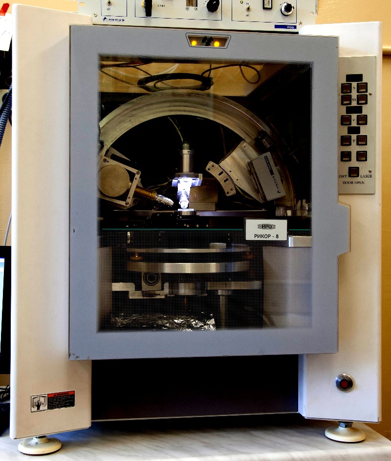
Multipurpose x-ray complex "RIKOR-8"
“RIKOR-8” is designed for the phase, structural, elemental analysis of crystalline, polycrystalline and amorphous samples. The unique feature of the device is the combination of the x-ray diffractometer and x-ray fluorescence spectrometer capabilities in one device.
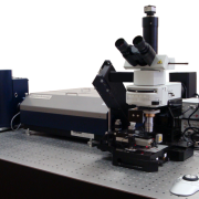
Laboratory complex for nanoelectronics elements development on the basis of local anodic oxidation
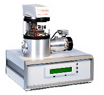
Laboratory complex is based on universal scanning probe microscope Solver-Pro (AFM, STM, samples diameter up to 100 mm). Equipped with a humidity control system, means of static electrical characteristics in-situ measurements.
Sputter coater Emitech K575X
Sputtering of ultra-thin films Au, Ag, Pd, Pt, Cr, Ti, Ta, Ni, etc. on the substrate up to 100 mm (4 inches) in diameter
The main procedure of analyser is based on the method of the adsorbate (nitrogen) thermal desorption in dynamic conditions. In this method, the fixed stream of helium-nitrogen (or other gas mixture) with adjusted structure passes through the adsorber with the sample.
Thus, the main area - is the study of porous nanostructures.