About
|
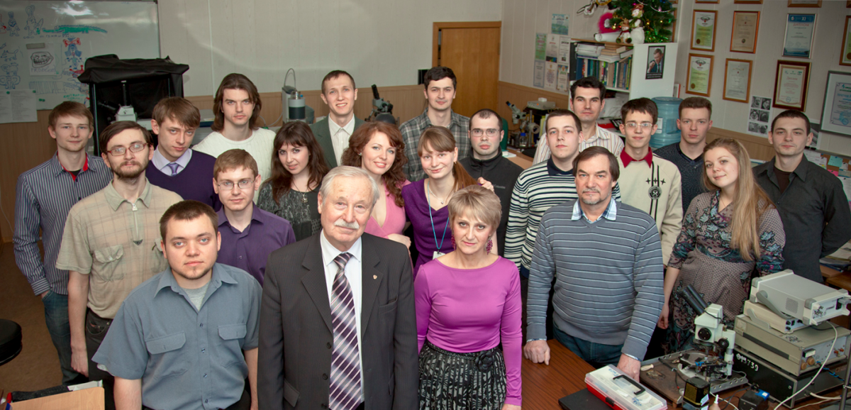
Center "Nanotechnology in electronics," was established in the State Educational Institution "Moscow Institute of Electronic Technology (Technical University)" in 2005 as a confirmation of the leading positions in the field of nanoelectronics MIET. Center works closely with the Teaching and Research Center "Probe microscopy and nanotechnology," created with the participation of "NT-MDT" in 1999 on the basis of laboratory tunneling microscopy and nanotechnology. The priority directions of scientific research of the Centre are: probe microscopy, nano probe, searching for new methods and materials to create nanoelectronics. (including AFM, TEM, FIB, MBE and Raman spectroscopy) A brief historical background among the first in Russia was built scanning tunneling microscope designed for technological experiments (AS number 1,471,232 on 14/07/87). In 1989 it was shown the presence of quantization of the conductivity at room temperature in a quasi-vertical conductors. In 1993 he built a tunnel microscope technology TTM-2, which yields atomic resolution structures. Created unique elements of nanoelectronics based on polymer, metal and carbon nanowires. The Center is currently active in investigating the properties of carbon nanotubes and nanoelectronic elements based on them. The center cooperates with companies and laboratories in MIET (plant "Proton" SRC "Technology Center", Electron Microscopy Laboratory, Department of Chemistry, etc.) that allows you to conduct comprehensive research on forced and scientific directions of the Centre. |