Molecular nanowires and organic electronics
Currently, one of the promising areas of science and industry is the development of photoactive devices based on organic materials. For example, OLED-technology makes it possible to convert electrical energy into radiation by using a special polymer phosphors to improve efficiency and durability of the device. However, despite the overall success in this area, there are still many difficulties, such as the fragility of devices due to the high rate of degradation.In order to improve the energy transfer, it was decided to use the special structure-based inks - J-aggregates of cyanine dyes, which are not only organized in a completely ordered structure, but also allow you to get a brand new photovoltaic properties such as high quantum yield and a high response extinction. These aggregates form different structures, such as tape, tube and film, and these structures may serve as a high-phosphors in photovoltaic devices. The most significant advantage of the proposed solution is a high energy output at low thickness and flexibility of the device.
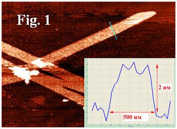
Thus, various experiments were conducted to study the properties of J-aggregates on different surfaces.Were carried out AFM measurements J-aggregates on various surfaces, including graphite, silicon and mica (Fig. 1 - mica). On mica, as shown in Fig. 1, the formation of nanoscale structures. Further studies were carried out in the direction of strengthening the aggregation by the promoters.
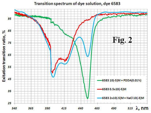
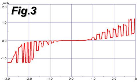
We investigated the absorption and luminescence spectra of dye aggregates in solution and on substrates (Fig. 2).As a result, experiments were conducted on the formation of the simplest structures to study the photoelectric properties of J-aggregates: on glass and silicon substrates with the wiring set up contacts were deposited film J-aggregates of cyanine dyes (the method of planting of the drop, centrifugation, and cross-dielectrophoresis).The results showed that the conductivity of the structure increases sharply (by 2-3 orders of magnitude) when exposed to light (Fig. 3). Thus, the structure can be used as sensitive to a specific emission spectrum of an optical sensor - matrix.